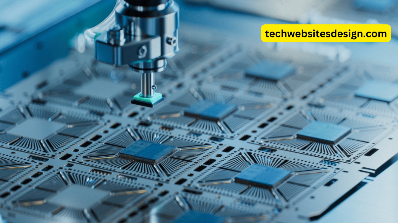
VLSI technology sits at the heart of a semiconductor revolution that’s reshaping our digital landscape. The industry has experienced unprecedented growth in the past few years, which reflects how VLSI semiconductors have become fundamental to everything from smartphones to autonomous vehicles.
When you examine the evolution of VLSI technology, you’ll notice how rapidly the field is advancing. Technology nodes in VLSI continue to shrink while capabilities expand, creating exciting opportunities for professionals and students alike. The future scope of VLSI technology offers tremendous potential. Furthermore, global investment in semiconductor manufacturing is accelerating, with India alone pushing for semiconductor self-reliance through investments worth billions of pounds. So, it is the best time to take a step and establish a career in this field.
Miniaturisation and Integration: The New Frontiers
Table of Contents
As traditional transistor architectures near their physical limits, VLSI technology is entering a new era of innovation.
- GAA Transistors:
A major shift from FinFETs, Gate-All-Around (GAA) transistors fully surround the channel, offering improved control, higher performance, and lower power consumption, core concepts in any modern VLSI design course. - Advanced Nodes (2nm and beyond):
Nanosheet-based designs pack more transistors into smaller spaces, but introduce challenges like increased quantum effects, higher costs, and defect rates. - New Materials:
Alternatives like GaN and SiC offer better thermal management and performance, while graphene and other 2D materials show promise for future transistor designs. - Chiplet Architecture:
Instead of monolithic chips, smaller specialised dies are used for better yield, flexibility, and cost-efficiency, an emerging trend in VLSI system design. - Beyond Moore’s Law:
With scaling limits in sight, the industry is turning to 3D integration and heterogeneous systems to maintain growth and innovation.
3D ICs and Packaging: Building Up, Not Out
As horizontal scaling approaches its physical limits, the semiconductor industry is shifting to 3D integrated circuits (ICs), which stack silicon layers vertically using through-silicon vias (TSVs). This architecture reduces the distance between compute and memory units, boosting bandwidth while cutting latency and power use. Unlike traditional chips, 3D ICs enable compact, high-performance systems with better scalability and support for heterogeneous integration. However, stacking increases power density, making heat management a key challenge, which is now addressed through advanced cooling methods and thermal-aware design. Complementing this trend is fan-out wafer-level packaging (FOWLP), which improves thermal efficiency and form factor. As VLSI technology advances, 3D integration is becoming central to driving performance beyond traditional transistor scaling.
AI and Automation in VLSI Design
Artificial intelligence is revolutionising how chip designers approach complex VLSI challenges. The marriage between AI and VLSI design represents a profound shift in semiconductor development methodologies.
AI now touches virtually every stage of the design process. Modern EDA tools harness AI to automate tasks that previously consumed countless engineering hours. These systems can predict design flaws, optimise layouts, and generate test patterns autonomously.
Tools like Synopsys DSO.ai use reinforcement learning to search massive solution spaces for optimal power, performance, and area configurations, exploring design alternatives far beyond human capability.
AI has also transformed verification, automating test pattern generation and identifying bugs efficiently. For students in a VLSI design course, understanding these AI-powered workflows is as fundamental as circuit design.
Generative AI tools like Synopsys.ai Copilot act as assistants, answering design methodology questions and creating workflow scripts through natural language. As they learn from usage, these systems evolve into tailored tools that accelerate design and improve quality.
AI also contributes to analogue design, expediting schematic migration between different process design kits. Across the VLSI semiconductor industry, AI is becoming a vital collaborator in tackling chip complexity and advancing technology nodes.
Conclusion
VLSI technology stands at the brink of transformative growth. As traditional scaling reaches limits, the industry advances through 3D integration, advanced packaging, and AI-driven design. This shift opens up exciting possibilities for those entering the field, making now an ideal time to pursue a VLSI course.
New technologies like GAA transistors, chiplet architectures, and heterogeneous integration demand professionals skilled in both foundational and emerging concepts. AI’s role in design is particularly game-changing, which is redefining how engineers solve complex problems.
Despite challenges like thermal issues and quantum effects, the semiconductor industry continues to innovate. For students, professionals, and industry leaders, the ability to merge core design knowledge with new technologies is key. VLSI will keep shaping the digital future, and those ready to evolve with it will lead the way.